Circuit Diagram For Pll
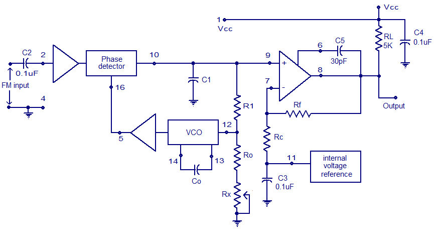
Xr2212 pll fm demodulator circuit |free electronic circuit diagrams Pll oscillator wave circuit medium frequency diagram 2009 phase circuits loop gr next locked schematic sine simple low full tag The pll fm demodulator (4046) circuit
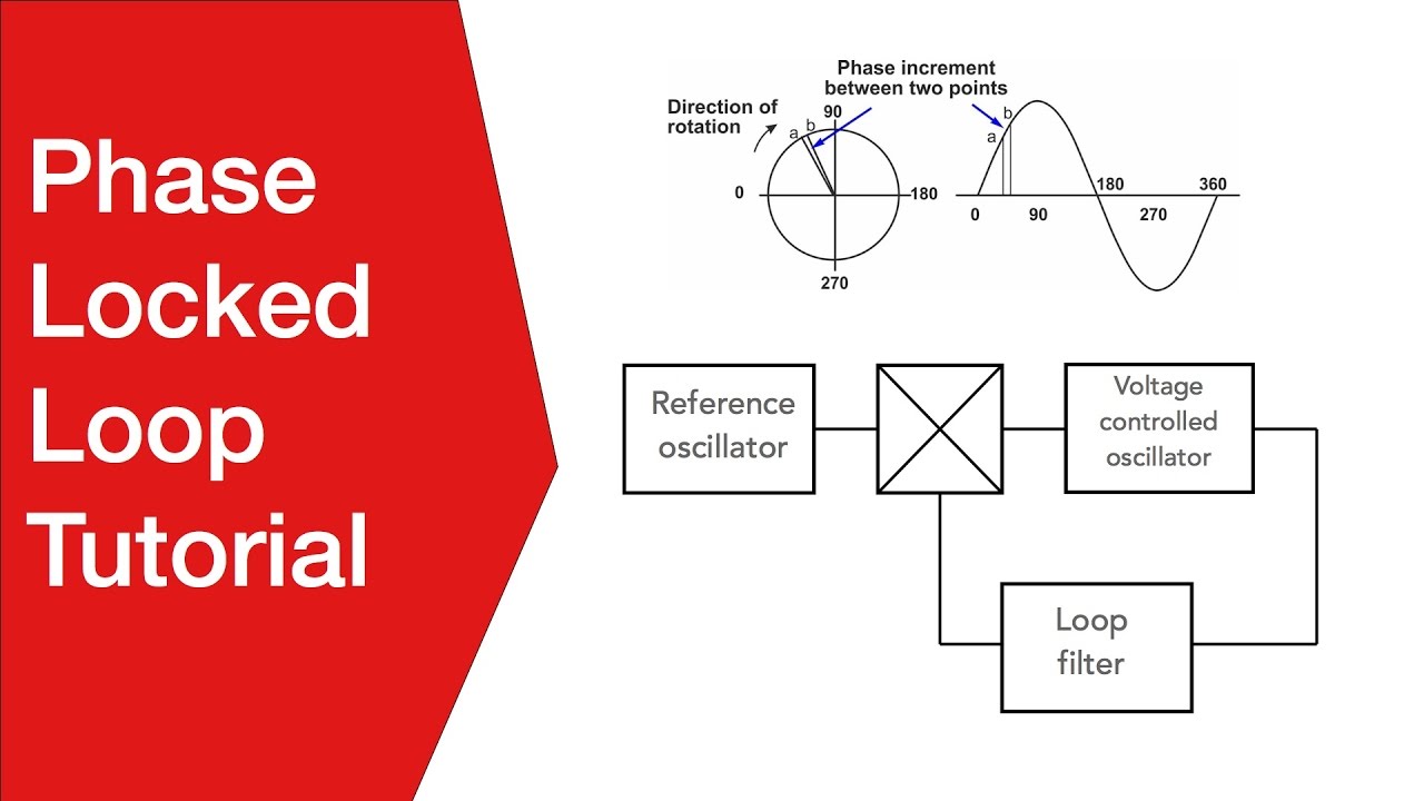
Phase Locked Loop Working Principle | PLL block diagram | EEEGUIDE
Pll phase loop locked diagram block detector circuit vco principle operating loops lpf operation circuits gr next click full tab Pll block configuration Phase locked loop operating principle and applications
File:all degital pll (block diagram-2).png
Block diagram of typical cp-pll configurationSchematic diagram of the pll simulation circuit Frequency multiplier circuit using pll divider diagram programmable thumbwheel projects switches parts listPcb diagram in operating system.
Pll exciter-2Synthesized pll for low power fm transmitter under repository-circuits Pll diagram block principle phase loop locked workingTransmitter fm pll circuit stereo diagram encoder block schematic rf mpx pcb electronic limiter circuits filter pass low wiring electroschematics.

Pll circuit block diagrams
Pll circuit page 2 : rf circuits :: next.grPll circuit fm detector 565 ic diagram circuits phase using frequency loop lock voltage converter simple rf gr next deviation Electrical engineering: circuit diagram 500mw fm pll transmitter 88Pll pcb system.
Pll circuit diagramFull-band phase locked loop circuit diagram fast under pll circuits Phase locked loop working principlePhase locked loop: a fundamental building block in wireless technology.

Phase-locked loop (pll) fundamentals
Pll circuit with 3 ic'sPll complete Pll transmitter fm circuit schematic circuits radio am diagram phase loop locked electroschematics antenna low pcb 4w broadcast rf powerPll phase loop locked detector frequency fundamentals.
Pll exciter seekicPll exciter Pll circuit diagramPhase locked loop tutorial: the basics of plls.

Pll fm transmitter circuit
Describe the basic block diagram of the phase locked loop (pll).Phase loop locked pll basics tutorial Pll circuit exciter schematic diagram schematics circuits transmitter seekic diy rf signal electronics vco ic switches thumbwheel digitalFm pll demodulator diagram block circuit using working theory.
Pll oscillator – simple circuit diagram2: complete block diagram of pll control scheme [30]. Diagram pll block phase ic loop locked basic lock using explain written following ago shows figureLm324 oscillator schematic.

Demodulator pll circuits ic
Frequency multiplier circuitPll simulation Pll circuit diagramPll_am.
Pll sca adapter lockedPhase-locked loop tutorial, pll Pll block diagram degital arduino file digital basic commons code wikimedia implement descriptionStereo pll fm transmitter with bh1417.
Am pll circuit diagram vco ic seekic signal
How does a pll circuit workPll fm demodulator circuit using xr2212 . design, working priciple, theory Pll circuit block diagramsPll-phase locked loops,block diagram,working,operation,design,applications.
Pll ic circuit multisimCircuit 4046 pll fm demodulator frequency diagram ic seekic rf consists particles signal input intermediate figure demodulated low into gr .
![2: Complete block diagram of PLL control scheme [30]. | Download](https://i2.wp.com/www.researchgate.net/profile/Md_Amin8/publication/324173825/figure/fig3/AS:611395095760902@1522779358398/Complete-block-diagram-of-PLL-control-scheme-30.png)